
Intel has began to innovate the semiconductor structure to strengthen the competitiveness of the foundry business. It has succeeded in developing next-generation technology that supplies power to drive semiconductors from the rear side of the wafer, which is a technology that improves bottlenecks and cell utilization of power and signal lines by arranging power wiring on the rear side of the wafer.
Intel announced on the fifth (local time) that it has implemented ‘PowerVia’ technology, which supplies power from the back of a semiconductor device, to a test chip. Intel is the primary within the semiconductor industry to implement backside power delivery technology.
The industry analyzed that Intel is aiming to recapture the foundry leadership through the introduction of the Powervia solution. Intel plans to use this technology starting with the Intel 20A process semiconductor, which is scheduled for mass production in the primary half of 2024.
Intel 20A is a semiconductor manufacturing process at the extent of two nanometers. It’s a method to alter the semiconductor industry by allowing Intel foundry service customers to utilize the technology.
Existing semiconductors used a frontside power delivery method that supplies power by applying wiring to the front side of the wafer on which circuits are drawn. Put the transistor at the underside, the ability wiring at the highest, after which the wiring that transmits the signal.
The front power supply has a limitation in that it occupies a big area since the signal transmission circuit and the ability supply wiring are co-located. Because the ability and signal lines utilize the identical resources, the connection line becomes a bottleneck problem. Signal and power wiring are mixed, which may easily generate noise, which negatively affects semiconductor performance. As well as, an enormous cost is consumed to expand the wiring layer as a consequence of the expansion of the transistor.
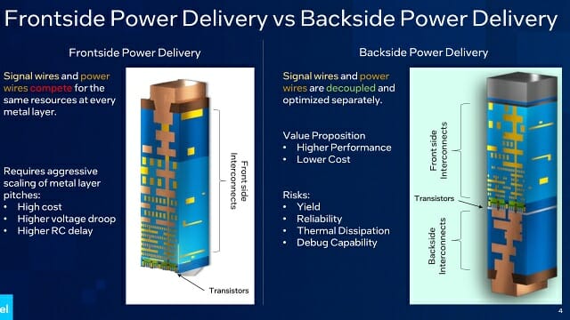
The facility via is a technique of leaving a structure wherein wires that provide signals and power are mixed, and wires that only send and receive signals at the highest of the transistor and provide power at the underside. The bottom line is to separate signal and power wires by supplying power from behind the wafer.
It is straightforward to know as an apartment. Previously, there have been power and signal lines in apartments on the twentieth floor, which made it difficult to transmit signals. Now, power lines are placed only within the basement and signal lines are placed only on the bottom floor, enabling efficient signal transmission.
Unlike the prevailing semiconductor structure, the bottleneck phenomenon is solved by changing the arrangement within the order of signal line-transistor-power line. As power lines are placed on the rear side of the wafer, the utilization rate of cells on the highest side of the wafer may also be improved. Since interference doesn’t occur, power efficiency may be increased and semiconductor performance may be improved.
Intel explained that by applying the PowerVia solution, it has achieved improvements resembling standard cell utilization of over 90%, clock speed of 6%, and platform voltage drop of greater than 30%.
‘Ribbon PET’, a next-generation transistor structure, can even be applied. Ribbon Pet is its own name for ‘Gate All Around (GAA)’, a technique wherein a gate surrounds a channel. In comparison with Finpet, which covers 3 sides, the contact side increases by 1 side. It is feasible to fine-tune the present to extend power efficiency.
The intention is to quickly meet up with the advanced semiconductor technique of TSMC and Samsung Electronics with Powervia and Ribbon Pet.
Ben Sell, vp of technology development at Intel, said, “We’re in a position to introduce rear power supply technology to the market one step ahead of competitors.” .
Intel plans to present the Powervia research results on the VLSI Symposium to be held in Kyoto, Japan from the eleventh to the sixteenth.
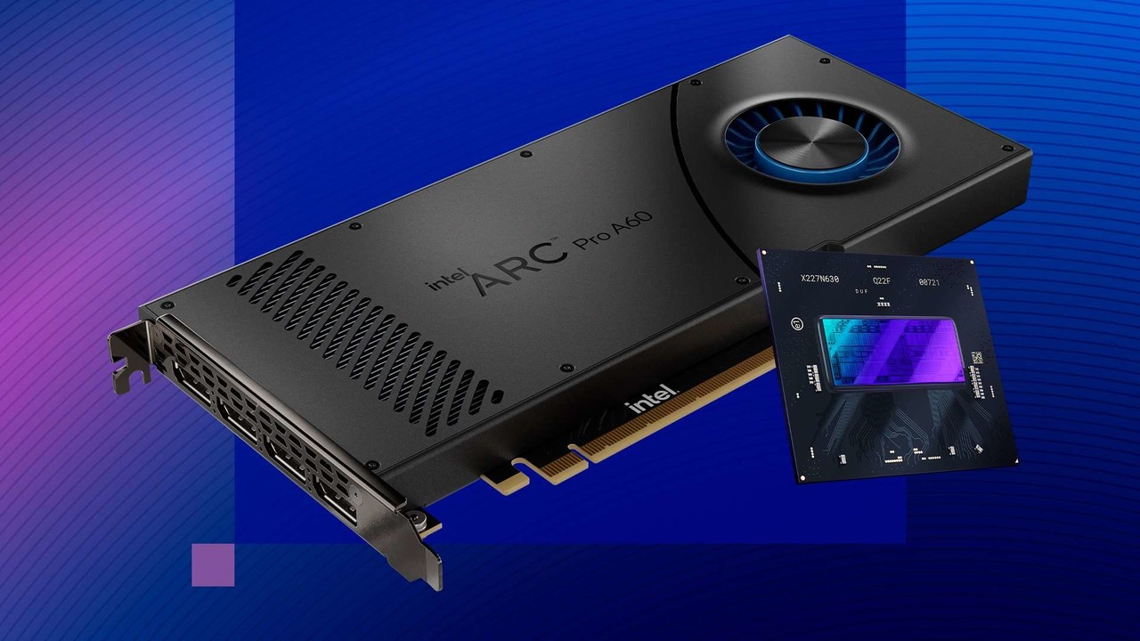
As well as, on the identical day, Intel also unveiled the Arc Pro A60 and Arc Pro A60M, the brand new products of the Intel Arc Pro A series skilled GPU.
The Intel Arc Pro GPU provides a working environment suitable for computer-aided design and modeling (CAD/CAM), AI inference tasks, and media data processing.
The Arc Pro A60 for desktop and the Arc Pro A60M for mobile support as much as 12GB of video memory (VRAM) and are designed for professionals who can connect as much as 4 displays that support High Dynamic Range (HDR) and Dolby Vision. The Arc Pro A60 GPU has built-in ray tracing hardware, graphics acceleration and machine learning capabilities. Along with this, it has integrated fluid viewports that support the most recent visualization technology and wealthy content creation in the prevailing single slot factor.
The Intel Arc Pro A60 and A60M feature as much as 16 PCIe lanes, 384 gigabytes per second memory bandwidth, 256 dedicated AI Xe Matrix Expansion (XMX) engines, 16 ray tracing units, CAD/CAM, AI inferencing and more. speed up The built-in media engine supports encoding and decoding of the most recent codecs resembling H.264/265 and AV1. The utmost power consumption is 130W, and the FP32 calculation performance is as much as 10.04PF (teraflops).
Arc Pro GPUs are designed for architectural and industrial applications including Autodesk’s 3ds Max, AutoCAD, Fusion, Inventor, Maya, Bentley Microstation, Dassault Systèmes SolidWorks, Nemechek Vectorworks, PTC Creo, Siemens’ NX and Solid Edge. Optimized.
Arc Pro A60-mounted graphics cards will likely be available in just a few weeks through major suppliers. Mobile workstations with A60M can even be released through major PC manufacturers.
Reporter Park Chan cpark@aitimes.com
smooth jazz
jazz music
sound of water
jazz instrumental